

Microcontroller Kits
Programmer and Target 89s51![]()
Simple Mikrokontroller 89s51 Trainer
Standart
Mikrokontroller 89s51 Trainer![]()
Super Mikrokontroller Trainer 89s51
All Item Include
1. Microcontroller MCS-51 Architecture
1.1. Memory Organization
All 80C51 devices have separate address spaces for program and data memory, as shown in Figures 1.1.1 and 1.1.2. The logical separation of program and data memory allows the data memory to be accessed by 8-bit addresses, which can be quickly stored and manipulated by an 8-bit CPU. Nevertheless, 16-bit data memory addresses can also be generated through the DPTR register. Program memory (ROM, EPROM) can only be read, not written to. There can be up to 64k bytes of program memory. In the 89s51, the lowest 4k bytes of program are on-chip. In the ROMless versions, all program memory is external. The read strobe for external program memory is the PSEN (program store enable).
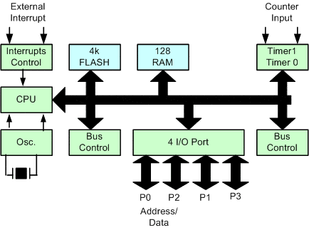
Figure 1.1.1 89s51 Block Diagram
Data Memory (RAM) occupies a separate address space from Program Memory. In the 80C51, the lowest 128 bytes of data memory are on-chip. Up to 64k bytes of external RAM can be addressed in the external Data Memory space. In the ROMless version, the lowest 128 bytes are on-chip. The CPU generates read and write signals, RD and WR, as needed during external Data
Memory accesses. External Program Memory and external Data Memory may be combined if desired by applying the RD and PSEN signals to the inputs of an AND gate and using the output of the gate as the read strobe to the external Program/Data memory.
Program Memory
Figure 1.1.4 shows a map of the lower part of the Program Memory. After reset, the CPU begins execution from location 0000H. As shown in Figure 1.1.4, each interrupt is assigned a fixed location in Program Memory. The interrupt causes the CPU to jump to that location, where it commences execution of the service routine. External Interrupt 0, for example, is assigned to location 0003H. If External Interrupt 0 is going to be used, its service routine must begin at location 0003H. If the interrupt is not going to be used, its service location is available as general purpose Program Memory.
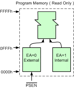
Figure 1.1.2. Memory Program Structure
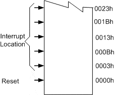
Figure 1.1.3. Interrupt Location
Data Memory
The right half of Figure 1.4 shows the internal and external Data Memory spaces available to the 80C51 user.The CPU generates RD and WR signals as needed during external RAM accesses. Internal Data Memory is mapped in Figure1.5. The memory space is shown divided into three blocks, which are generally referred to as the Lower 128, the Upper 128, and SFR space.
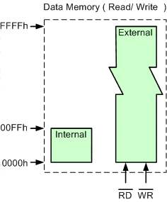
Figure 1.1.4. Memory Data Structure
Internal Data Memory addresses are always one byte wide, which implies an address space of only 256 bytes. However, the addressing modes for internal RAM can in fact accommodate 384 bytes, using a simple trick. Direct addresses higher than 7FH access one memory space, and indirect addresses higher than 7FH access a different memory space. Thus Figure 1.1.5. shows the Upper 128 and SFR space occupying the same block of addresses, 80H through FFH, although they are physically separate entities.
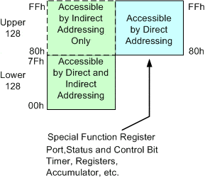
Figure 1.5. Internal Data Memory
The Lower 128 bytes of RAM are present in all 80C51 devices as mapped in Figure 1.1.6. The lowest 32 bytes are grouped into 4 banks of 8 registers. Program instructions call out these registers as R0 through R7. Two bits in the Program Status Word (PSW) select which register bank is in use. This allows more efficient use of code space, since register instructions are shorter than instructions that use direct addressing.
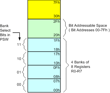
Figure 1.1.6. Lower 128 bytes of internal RAM
All of the bytes in the Lower 128 can be accessed by either direct or indirect addressing. The Upper 128 (Figure 1.1.7) can only be accessed by indirect addressing.
Figure 1.1.7.Upper 128 Bytes of Internal RAM